Find your way to our products

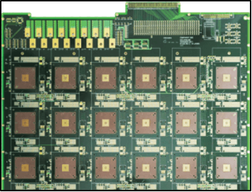
HDI PCB

Socket PCB

Rigid Flexible PCB

Load PCB

Special PCB
Burn-In PCB

Flexible PCB

MLO PCB

MLB PCB

PCB Capability
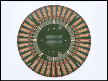
Probe Card PCB
PCB Lead Time
PCB trouble?
EDINS solved this
When you meet EDINS, all your PCB purchase worries are solved.


HDI PCB
Layer : ~32L Aspect ratio 11:1
Bind, Buried, Stack and HPL(Hole Plugging Land)
Production lead time 3~15 days
Wide material selection ranges FR-4 High Tg, Rogers, ISOLA, Panasonic(Halogen free) and Taconic
Board thickness 0.1mm ~ 3.2mm
Min Track / Gap/ Inner layer 40um / 40um(Special) / 60um / 80um(STD)
Outer layer 75um / 75um(Special) / 100um / 100um(STD)
Min hole diameter 0.15ø / 0.1ø (Mechanical / Laser) 0.1ø (stack via)
Micro via / Pad size 0.1ø / 270um
Rigid-Flex PCB
Design consulting
Blind / Buried via
SMD Assembly Possible!
Stack via Layers up to 16L
Cu Thickness(RA / ED) : 9㎛ ~ 70㎛
Dimension : 500mm X 700mm
Impedance control : 50Ω ± 7%
Min. Track & Gap : 50㎛ / 50㎛
Edge to pattern clearance:100㎛


Special PCB
Layers up to 80 Blind / Buried via
Aspect ratio 26.6:1 Stack via POV(Pad On Via)
Dimension(Diameter) :~650mm
Board thickness : 4.5mm ~ 8.0mm
Flatness : ± 200㎛
Thickness tolerance :150㎛
Impedance control : 50Ω ± 7%(5%, if Special) Surface Finish
ENEPIG : Electroless Ni + Electroless Pd + Imm. Ni / Au
Thick ENIG : Ni – 4~8㎛ / Au – 0.5~0.8㎛
Flexible PCB
COF & Flip chip scales
SMD Assembly Possible!
Layers up to 12L
Cu Thickness(RA / ED) : 9㎛ ~ 70㎛
Dimension : 500mm X 700mm / Roll-to-Roll
Min. Track & Gap : 25㎛ / 25㎛
Min. pattern to via clearance : 50㎛
Edge to pattern clearance:100㎛


MLB PCB
Layer : ~ 50
Thickness : 6.2 mm
Material : FR-4(H) & etc
Size : ~ 550 x 750 mm
Via on pad / BVH ( Blind & Buried )
MLB & Build-up